
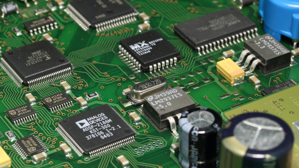
A Multi-Layer PCB is a type of printed circuit board that contains more than two layers of conductive material, allowing for highly complex and dense circuit designs. These boards are made by stacking multiple layers of PCBs, each separated by insulating layers, and then interconnecting them through vias (holes that are drilled and plated to allow electrical connections between layers).
Key Features:
- Multiple Layers: Multi-layer PCBs typically have three or more layers of conductive material, providing more space for intricate circuit designs. These layers can be used to route signal, power, or ground connections.
- High-Density Interconnect: The additional layers allow for more components to be placed within a smaller footprint, increasing circuit density and enabling more complex
- Inner and Outer Layers: The outer layers typically contain components and traces visible on the surface, while the inner layers handle additional circuitry, which can be used for power, ground planes, or signal routing.
- Vias and Through-Hole Plating: Interlayer connections are made using vias, which are drilled holes that are plated with copper to create electrical pathways between layers.
Applications:
- High-Performance Consumer Electronics: Multi-layer PCBs are essential for advanced electronic devices such as smartphones, laptops, tablets, and high-end audio systems, where space is limited and performance needs are high.
- Medical Devices: Devices like MRI machines, pacemakers, and diagnostic equipment require multi-layer PCBs for their intricate and precise electronic needs.
- Telecommunications: Multi-layer PCBs are widely used in telecommunications equipment like servers, base stations, and networking hardware where high-speed signal transmission is crucial.
- Automotive Electronics: In modern vehicles, multi-layer PCBs are used in critical systems such as infotainment, GPS, safety features, and electric vehicle components.
- Aerospace and Military Applications: Aerospace and defense systems require multi-layer PCBs for complex, mission-critical electronics used in navigation, communication, radar, and flight control systems.
- Industrial Automation: Multi-layer PCBs are used in robotics, control systems, and industrial machinery where space optimization and performance are essential.
Advantages:
- Increased Circuit Density: Multi-layer PCBs allow for a significant increase in the number of components and connections within a smaller footprint, which is ideal for compact
- Improved Performance: With better routing capabilities and the ability to separate power, ground, and signal layers, multi-layer PCBs can reduce noise, signal interference, and improve overall circuit performance.
- Smaller Form Factor: By stacking layers, designers can fit complex circuits into smaller, more compact sizes, which is critical for today’s miniaturized electronic devices.
- Enhanced Reliability: Multi-layer PCBs are more robust and durable, with better heat dissipation and the ability to handle high-frequency signals more effectively.
Multi-Layer PCBs are the go-to solution for high-performance, compact, and reliable electronics. They are ideal for applications where the complexity of the circuit exceeds the capabilities of single- or double-sided PCBs, and where space and performance are both critical. Though more expensive and complex to manufacture, their benefits in terms of circuit density, signal integrity, and overall performance make them indispensable in modern electronic devices.